PCB Jam digital dengan P16F84A MCU, click gambar untuk memperbesar
Daftar Belanja (semua resistor 0.25 watt)
Resistor
R1-R7 (7 buah) 330 Ohm
R8-R11 (4 buah) 4k7 Ohm
R12-R14 (3 buah) 10k Ohm
Capasitor
C1 100uF, 16Volt elektrolit
C2 100nF Ceramic
C3-C4 (2buah) 33pF Ceramic
LED display
7 Segment (4 buah) Common Anoda
Dioda
D1 - D2 (2buah) Schottky 1N5817
D3 1N4001
Transistor
Q1-Q4 (4buah) BC 557 atau PNP lainnya
MCU
Microcontroller P16F84a
Lain - Lain
X'tal 4 Mhz
Socket IC 18 pin DIL
Battery Holder CR 2023
Battery CR 2023 Lithium 3 Volt
s1- s2 (dua buah) Push Button (saklar tekan)
DC plug jantan + betina untuk koneksi dengan catu daya
Kabel Kaku untuk jumper secukupnya
kabel untuk catu daya secukupnya
Komponen harus dipasang sependek mungkin. Saya tidak memasangkan kapasitor elektrolit C1 dalam posisi "berdiri" melainkan dalam posisi tidur, agar tidak terlalu tinggi. Dengan memasang komponen sependek mungkin nantinya akan memudahkan PCB dipasang pada panel tanpa "terganjal" oleh komponen. Perhatikan pula ada 4 buah jumper pada PCB.
Sebaiknya jam digital ini dipasang dalam box atau lukisan agar indah dipandang. Selanjutnya jam digital ini perlu Catu Daya dengan tegangan 5 Volt stabil. Bila anda belum mempunyai catu daya, maka anda dapat merakitnya sendiri! Artikel tentang catu daya yang distabilkan akan segera menyusul. Selamat bekerja. Semoga sukses!!
Bila anda ingin paket lengkap komponen jam digital (termasuk MCU yang telah diprogram dan PCB, tidak termasuk kabel dan catu daya), anda dapat memesan kepada saya. Harganya Rp 120 ribu saja (belum termasuk ongkos kirim). Hubungi saya, kontak sms HP: 0229 919 313 28. Silahkan kirim pertanyaan, komentar, koreksi atau apa saja pada form di bawah. Terima kasih!
http://gemar-elektronika.com/hastakarya/jam-digital.html?start=3


RF TRANSMITTER AND RECEIVER SECTION
INTRODUCTION
Radio frequency (RF) usually refers to oscillations in electrical circuits. It is normally use in wireless communication system to transmit data. By modulating data signals onto the RF carrier signal, data can be transfer from one point to the other point easily. In this application note, a pair of RF module with a frequency of 433 MHz is used.
To interface RF module with microcontroller, Universal Synchronous and Asynchronous Receiver and Transmitter (USART) or also known as Serial Communications Interface is used. USART is used for transmit and receive serial data. The operation of USART can be divided into two types which is synchronous and asynchronous. Synchronous mode uses a clock and data line. Asynchronous mode does not use clock accompanying the data. However in this application note, only asynchronous mode will be use in interfacing the RF module with the microcontroller.
BLOCK DIAGRAM
TRANSMITTER SECTION
OBJECTIVE
Interface a RF module with microcontroller to build a wireless remote control.
HARDWARE
1. Transmitter Encoder
2. RF Transmitter
TRANSMITTER ENCODER
A encoder is a device, circuit, transducer, software program, algorithm or person that converts information from one format or code to another, for the purposes of standardization, speed, secrecy, security, or saving space by shrinking size.
TRANSMITTER ENCODER HT12E
The HT12E encoders are a series of CMOS LSIs for remote control system applications. They are capable of encoding information which consists of N address bits and 12_N data bits. Each address/ data input can be set to one of the two logic states. The programmed addresses/data are transmitted together with the header bits via an RF or an infrared transmission medium upon receipt of a trigger signal. The capability to select a TE trigger on the HT12E or a DATA trigger on the HT12A further enhances the application flexibility of the 212 series of encoders.

Features of HT12E
Ø Operating voltage 2.4V~12V
Ø Low power and high noise immunity CMOS technology
Ø Low standby current: 0.1_A (typ.) at VDD=5V
Ø Minimum transmission word
Ø Four words for the HT12E
Ø One word for the HT12A
Ø Built-in oscillator needs only 5% resistor
Ø Data code has positive polarity
Ø Minimal external components
fig: HT12E interfacing with transmitter
PIN DESCRIPTION OF HT12E-18DIP
Electrical Characteristics of HT12E
Absolute Maximum Ratings
Supply Voltage -0.3V to 13V
Storage Temperature -50C to 125C
Operating Temperature -20C to 75C
Note: These are stress ratings only. Stresses exceeding the range specified under Absolute Maximum Ratings may cause substantial damage to the device. Functional operation of this device at other conditions beyond those listed in the specification is not implied and prolonged exposure to extreme conditions may affect device reliability.
Available packages

Functional Description
Flow chart
Operation

The 212 series of encoders begin a 4-word transmission cycle upon receipt of a transmission enable (TE for the HT12E or D8~D11 for the HT12A, active low). This cycle will repeat itself as long as the transmission enable (TE or D8~D11) is held low. Once the transmission enable returns high the encoder output completes its final cycle and then stops as shown below.
Fig: Transmission timing for the HT12E
Address/data waveform
Each programmable address/data pin can be externally set to one of the following two logic states as shown below. The address/data bits of the HT12A are transmitted with a 38 kHz carrier for infrared remote controller flexibility.

Fig: Address/Data bit waveform for the HT12E
Address/data programming
The status of each address/data pin can be individually pre-set to logic high or low. If a transmission enable signal is applied, the encoder scans and transmits the status of the 12 bits of address/data serially in the order A0 to AD11 for the HT12E encoder and A0 to D11 for the HT12A encoder. During information transmission these bits are transmitted with a preceding synchronization bit. If the trigger signal is not applied, the chip enters the standby mode and consumes a reduced current of less than 1_A for a supply voltage of 5V. Usual applications preset the address pins with individual security codes using DIP switches or PCB
Wiring, while the data is selected by push buttons or electronic switches. The following figure shows an application using the HT12E

Applications
Ø Burglar alarm system
Ø Smoke and fire alarm system
Ø Garage door controllers
Ø Car door controllers
Ø Car alarm system
Ø Security system
Ø Cordless telephones
Ø Other remote control systems
RF TRANSMITTER
Overview
The STT-433 is ideal for remote control applications where low cost and longer range is required. The transmitter operates from a 1.5-12V supply, making it ideal for battery-powered applications. The transmitter employs a SAW-stabilized oscillator, ensuring accurate frequency control for best range performance. Output power and harmonic emissions are easy to control, making FCC and ETSI compliance easy. The manufacturing-friendly SIP style package and low-cost make the STT-433 suitable for high volume
Fig : Tx433 IC Image
Specifications of STT-433
Ø Frequency Range: 433.92MHZ
Ø Modulate Mode: ASK
Ø Circuit Shape: SAW
Ø Data Rate: 8kbps
Ø Supply Voltage: 3~12V
Ø Power Supply and All Input / Out Pins: -0.3 to +12.0v
Ø Non-Operating Case Temperature: -20 to 85C
Ø Soldering Temperature (10 Seconds): 230C( 10 Seconds )

Pin Description of TX433
Electrical characteristics, T=25c, Vcc=3.6v, Freq=433.92MHZ
Operation
OOK(On Off Keying) modulation is a binary form of amplitude modulation. When a logical 0 (data line low) is being sent, the transmitter is off, fully suppressing the carrier. In this state, the transmitter current is very low, less than 1mA. When a logical 1 is being sent, the carrier is fully on. In this state, the module current consumption is at its highest, about 11mA with a 3V power supply. OOK is the modulation method of choice for remote control applications where power consumption and cost are the primary factors. Because OOK transmitters draw no power when they transmit a 0, they exhibit significantly better power consumption than FSK transmitters. OOK data rate is limited by the start-up time of the oscillator. High-Q oscillators which have very stable center frequencies take longer to start-up than low-Q oscillators. The start-up time of the oscillator determines the maximum data rate that the transmitter can send.
Data Rate
The oscillator start-up time is on the order of 40uSec, which limits the maximum data rate to 4.8 kbit/sec.
SAW stabilized oscillator
The transmitter is basically a negative resistance LC oscillator whose center frequency is tightly controlled by a SAW resonator. SAW (Surface Acoustic Wave) resonators are fundamental frequency devices that resonate at frequencies much higher than crystals.
INTERFACING WITH HT12E

RECEIVER SECTION
OBJECTIVE
Interface a RF module with microcontroller to build a wireless remote control.
HARDWARE
1. RF Receiver
2. Receiver Decoder
RF RECEIVER STR-433
Overview
The STR-433 is ideal for short-range remote control applications where cost is a primary concern. The receiver module requires no external RF components except for the antenna. It generates virtually no emissions, making FCC and ETSI approvals easy. The super-regenerative design exhibits exceptional sensitivity at a very low cost. The manufacturing-friendly SIP style package and low-cost make the STR-433 Suitable for high volume applications.
Fig : Rx433 front view Fig : Rx433 Back view
FEATURES
Ø Low Cost
Ø 5V operation
Ø 3.5mA current drain
Ø No External Parts are required
Ø Receiver Frequency: 433.92 MHZ
Ø Typical sensitivity: -105dBm
Ø IF Frequency: 1MHz
Specifications
Pin Outs
Parameter Symbol Min Typ. Max Unit
Operation
Super-Regenerative AM Detection
The STR-433 uses a super-regenerative AM detector to demodulate the incoming AM carrier. A super regenerative detector is a gain stage with positive feedback greater than unity so that it oscillates. An RC-time constant is included in the gain stage so that when the gain stage oscillates, the gain will be lowered over time proportional to the RC time constant until the oscillation eventually dies. When the oscillation dies, the current draw of the gain stage decreases, charging the RC circuit, increasing the gain, and ultimately the oscillation starts again. In this way, the oscillation of the gain stage is turned on and off at a rate set by the RC time constant. This rate is chosen to be super-audible but much lower than the main oscillation rate. Detection is accomplished by measuring the emitter current of the gain stage. Any RF input signal at the frequency of the main oscillation will aid the main oscillation in restarting. If the amplitude of the RF input increases, the main oscillation will stay on for a longer period of time, and the emitter current will be higher. Therefore, we can detect the original base-band signal by simply low-pass filtering the emitter current.
The average emitter current is not very linear as a function of the RF input level. It exhibits a 1/in response because of the exponentially rising nature of oscillator start-up. The steep slope of a logarithm near zero results in high sensitivity to small input signals.
Data Slicer
The data slicer converts the base-band analog signal from the super-regenerative detector to a CMOS/TTL compatible output. Because the data slicer is AC coupled to the audio output, there is a minimum data rate. AC coupling also limits the minimum and maximum pulse width. Typically, data is encoded on the transmit side using pulse-width modulation (PWM) or non-return-to-zero (NRZ).
The most common source for NRZ data is from a UART embedded in a micro-controller. Applications that use NRZ data encoding typically involve microcontrollers. The most common source for PWM data is from a remote control IC such as the HC-12E from Holtek or ST14 CODEC.
Data is sent as a constant rate square-wave. The duty cycle of that square wave will generally be either 33% (a zero) or 66% (a one). The data slicer on the STR-433 is optimized for use with PWM encoded data, though it will work with NRZ data if certain encoding rules are followed.
Power Supply
The STR-433 is designed to operate from a 5V power supply. It is crucial that this power supply be very quiet. The power supply should be bypassed using a 0.1uF low-ESR ceramic capacitor and a 4.7uF tantalum capacitor. These capacitors should be placed as close to the power pins as possible. The STR- 433 is designed for continuous duty operation. From the time power is applied, it can take up to 750mSec for the data output to become valid.
Antenna Input
It will support most antenna types, including printed antennas integrated directly onto the PCB and simple single core wire of about 17cm. The performance of the different antennas varies. Any time a trace is longer than 1/8th the wavelength of the frequency it is carrying, it should be a 50 ohm microstrip.
Interfacing STR 433 with HT12D

Applications
Ø Car security system
Ø Sensor reporting
Ø Automation system
Ø Remote Keyless Entry (RKE)
Ø Remote Lighting Controls
Ø On-Site Paging
Ø Asset Tracking
Ø Wireless Alarm and Security Systems
Ø Long Range RFID
Ø Automated Resource Management
RECEIVER DECODER
A decoder is a device, circuit, transducer, software program, algorithm or person that converts information from one format or code to another, for the purposes of standardization, speed, secrecy, security, or saving space by shrinking size.
RECEIVER DECODER HT12D
Overview
The 212 decoders are a series of CMOS LSIs for remote control system applications. They are paired with Holtek_s 212 series of encoders (refer to the encoder/decoder
cross reference table). For proper operation, a pair of encoder/decoder with the same number of addresses and data format should be chosen. The decoders receive serial addresses and data from a programmed 212 series of encoders that are transmitted by a carrier using an RF or an IR transmission medium. They compare the serial input data three times continuously
with their local addresses. If no error or unmatched codes are found, the input data codes are
decoded and then transferred to the output pins. The VT pin also goes high to indicate a valid transmission. The 212 series of decoders are capable of decoding information’s that consist of N bits of address and 12_N bits of data. Of this series, the HT12D is arranged to provide 8 address bits and 4 data bits, and HT12F is used to decode 12 bits of address information
Features
Ø Operating voltage: 2.4V~12V
Ø Low power and high noise immunity CMOS
Ø technology
Ø Low standby current
Ø Capable of decoding 12 bits of information
Ø Binary address setting
Ø Received codes are checked 3 times
Ø Address/Data number combination HT12D: 8 address bits and 4 data bits
Ø Built-in oscillator needs only 5% resistor
Ø Valid transmission indicator
Ø Easy interface with an RF or an infrared transmission medium
Ø Minimal external components
Ø 18-pin DIP, 20-pin SOP package
Pin description
Functional Description
Operation
The 212 series of decoders provides various combinations of addresses and data pins in different packages so as to pair with the 212 series of encoders. The decoders receive data that are transmitted by an encoder and interpret the first N bits of code period as addresses and the last 12_N bits as data, where N is the address code number. A signal on the DIN pin activates the oscillator which in turn decodes the incoming address and data. The decoders will then check the received address three times continuously. If the received address codes all match the contents of the decoders local address, the 12_N bits of data are decoded to activate the output pins and the VT pin is set high to indicate a valid transmission. This will last unless the address code is incorrect or no signal is received. The output of the VT pin is high only when the transmission is valid. Otherwise it is always low.
Decoder timings

Output type
Of the 212 series of decoders, the HT12F has no data output pin but its VT pin can be used as a momentary data output. The HT12D, on the other hand, provides 4 latch type data pins whose data remain unchanged until new data are received.
Flowchart
The oscillator is disabled in the standby state and activated when a logic high signal applies to the DIN pin. That is to say, the DIN should be kept low if there is no signal input.
Interfacing HT12D With STR 433
Applications
Car security system
Wireless security systems
Sensor reporting
Automation system
Remote Keyless entry
Radio frequency (RF) usually refers to oscillations in electrical circuits. It is normally use in wireless communication system to transmit data. By modulating data signals onto the RF carrier signal, data can be transfer from one point to the other point easily. In this application note, a pair of RF module with a frequency of 433 MHz is used.
To interface RF module with microcontroller, Universal Synchronous and Asynchronous Receiver and Transmitter (USART) or also known as Serial Communications Interface is used. USART is used for transmit and receive serial data. The operation of USART can be divided into two types which is synchronous and asynchronous. Synchronous mode uses a clock and data line. Asynchronous mode does not use clock accompanying the data. However in this application note, only asynchronous mode will be use in interfacing the RF module with the microcontroller.
BLOCK DIAGRAM
 |
TRANSMITTER SECTION
OBJECTIVE
Interface a RF module with microcontroller to build a wireless remote control.
HARDWARE
1. Transmitter Encoder
2. RF Transmitter
TRANSMITTER ENCODER
A encoder is a device, circuit, transducer, software program, algorithm or person that converts information from one format or code to another, for the purposes of standardization, speed, secrecy, security, or saving space by shrinking size.
TRANSMITTER ENCODER HT12E
The HT12E encoders are a series of CMOS LSIs for remote control system applications. They are capable of encoding information which consists of N address bits and 12_N data bits. Each address/ data input can be set to one of the two logic states. The programmed addresses/data are transmitted together with the header bits via an RF or an infrared transmission medium upon receipt of a trigger signal. The capability to select a TE trigger on the HT12E or a DATA trigger on the HT12A further enhances the application flexibility of the 212 series of encoders.

Features of HT12E
Ø Operating voltage 2.4V~12V
Ø Low power and high noise immunity CMOS technology
Ø Low standby current: 0.1_A (typ.) at VDD=5V
Ø Minimum transmission word
Ø Four words for the HT12E
Ø One word for the HT12A
Ø Built-in oscillator needs only 5% resistor
Ø Data code has positive polarity
Ø Minimal external components
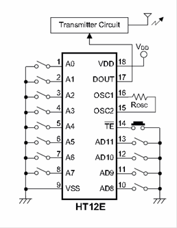
fig: HT12E interfacing with transmitter
PIN DESCRIPTION OF HT12E-18DIP
 |
| Pin No | Pin Name | Input/Output | Internal Connection | Description |
| 01~08 | A0 ~ A7 | Input | Nmos TransmissionGate Protection Diode | Input pins for address A0~A7 settingThese pins can be externally set to VSS or left open |
| 09 | Vss | Input | Negative power supply, grounds | |
| 10~13 | AD ~AD11 | Input | Nmos TransmissionGate ProtectionDiode and CMOS IN Pull-high |
Input pins for address/data AD8~AD11 setting. These pins can be externally set to VSS or left open and D8~D11 setting and transmission enable, active low These pins should be externally set to VSS or left open |
| 14 | TE | Input | CMOS IN Pull-high | Transmission enable, active low |
| 15 | OSC1 | Input | OSCILLATOR 1 | Oscillator input pin |
| 16 | OSC2 | Output | OSCILLATOR 1 | Oscillator output pin |
| 17 | Dout | Output | CMOS OUT | Encoder data serial transmission output |
| 18 | VDD | INPUT | Positive power supply |
| Symbol | Parameter | Test conditions | Min. | Typ. | Max. | Unit | |
| VDD | Conditions | ||||||
| VDD | Operating Voltage | 2.4 | 5 | 12 | v | ||
| ISTE | Standby Current | 3v | Oscillator Stops | 0.1 | 1 | µA | |
| 12v | 2 | 4 | µA | ||||
| IDD | Operating current | 3v | No load FOSC-3kHz | 40 | 80 | µA | |
| 2v | 150 | 300 | µA | ||||
| IDOUT | Output drive current | 5v | VOH=0.9VDD (Source) | -1 | -1.6 | mA | |
| VOL=0.1VDD (Sink) | 1 | 1.6 | mA | ||||
| VIH | “Input Voltage | 0.8VDD | VDD | V | |||
| VIL | “Input Voltage | 0 | 0.2VDD | V | |||
| FOSC | Oscillator Frequency | 5V | ROSC=1.1M | 3 | kHz | ||
| RTE’ | TE Pull-high Resistance | 5v | VTE’ =0V | 1.5 | 3 | MΩ | |
Supply Voltage -0.3V to 13V
Storage Temperature -50C to 125C
Operating Temperature -20C to 75C
Note: These are stress ratings only. Stresses exceeding the range specified under Absolute Maximum Ratings may cause substantial damage to the device. Functional operation of this device at other conditions beyond those listed in the specification is not implied and prolonged exposure to extreme conditions may affect device reliability.
Available packages

Functional Description
Flow chart
 |

The 212 series of encoders begin a 4-word transmission cycle upon receipt of a transmission enable (TE for the HT12E or D8~D11 for the HT12A, active low). This cycle will repeat itself as long as the transmission enable (TE or D8~D11) is held low. Once the transmission enable returns high the encoder output completes its final cycle and then stops as shown below.
Fig: Transmission timing for the HT12E
Address/data waveform
Each programmable address/data pin can be externally set to one of the following two logic states as shown below. The address/data bits of the HT12A are transmitted with a 38 kHz carrier for infrared remote controller flexibility.

Fig: Address/Data bit waveform for the HT12E
Address/data programming
The status of each address/data pin can be individually pre-set to logic high or low. If a transmission enable signal is applied, the encoder scans and transmits the status of the 12 bits of address/data serially in the order A0 to AD11 for the HT12E encoder and A0 to D11 for the HT12A encoder. During information transmission these bits are transmitted with a preceding synchronization bit. If the trigger signal is not applied, the chip enters the standby mode and consumes a reduced current of less than 1_A for a supply voltage of 5V. Usual applications preset the address pins with individual security codes using DIP switches or PCB
Wiring, while the data is selected by push buttons or electronic switches. The following figure shows an application using the HT12E

Applications
Ø Burglar alarm system
Ø Smoke and fire alarm system
Ø Garage door controllers
Ø Car door controllers
Ø Car alarm system
Ø Security system
Ø Cordless telephones
Ø Other remote control systems
RF TRANSMITTER
Overview
The STT-433 is ideal for remote control applications where low cost and longer range is required. The transmitter operates from a 1.5-12V supply, making it ideal for battery-powered applications. The transmitter employs a SAW-stabilized oscillator, ensuring accurate frequency control for best range performance. Output power and harmonic emissions are easy to control, making FCC and ETSI compliance easy. The manufacturing-friendly SIP style package and low-cost make the STT-433 suitable for high volume
 |
 |
Specifications of STT-433
Ø Frequency Range: 433.92MHZ
Ø Modulate Mode: ASK
Ø Circuit Shape: SAW
Ø Data Rate: 8kbps
Ø Supply Voltage: 3~12V
Ø Power Supply and All Input / Out Pins: -0.3 to +12.0v
Ø Non-Operating Case Temperature: -20 to 85C
Ø Soldering Temperature (10 Seconds): 230C( 10 Seconds )

Pin Description of TX433
| Pin No | Pin Description | Description |
| Pin No 1 | Ground | Transmitter ground. Connect to ground plane. |
| Pin No 2 | Data In | Digital data input. This input is CMOS compatible and should be driven with CMOS level inputs. |
| Pin No 3 | Vcc | Operating voltage for the transmitter. VCC should be bypassed with a .01uF ceramic capacitor and filtered with a 4.7uF tantalum capacitor. Noise on the power supply will degrade transmitter noise performance. |
| Pin No 4 | Antenna | 50 ohm antenna output. The antenna port impedance affects output power and harmonic emissions. An L-C low-pass filter may be needed to sufficiently filter harmonic emissions. Antennacan be single core wire of approximately 17cm length or PCB trace antenna. |
| Characteristic | Sym | Min. | Typ. | Max. | Uint |
| Operating Frequency (200Khz) | Vcc | 433.92 | MHZ | ||
| Data Rate | ASK | 100 | Kbps | ||
| TransmitterPerformance (ook@2.4kbps) | |||||
| Peak Input Current, 12 Vdc Supply | ITP | 45 | mA | ||
| Peak Output Power | Po | 10 | mW | ||
| Turn on / Turn Off Time | T ON / T OFF | 1 | us | ||
| Power Supply Voltage range | Vcc | mA | |||
| Operating Ambient Temperature | TA | -20 | +85 | C | |
| Tx Antenna Out(3V) +2.4dB | Vcc | mA |
OOK(On Off Keying) modulation is a binary form of amplitude modulation. When a logical 0 (data line low) is being sent, the transmitter is off, fully suppressing the carrier. In this state, the transmitter current is very low, less than 1mA. When a logical 1 is being sent, the carrier is fully on. In this state, the module current consumption is at its highest, about 11mA with a 3V power supply. OOK is the modulation method of choice for remote control applications where power consumption and cost are the primary factors. Because OOK transmitters draw no power when they transmit a 0, they exhibit significantly better power consumption than FSK transmitters. OOK data rate is limited by the start-up time of the oscillator. High-Q oscillators which have very stable center frequencies take longer to start-up than low-Q oscillators. The start-up time of the oscillator determines the maximum data rate that the transmitter can send.
Data Rate
The oscillator start-up time is on the order of 40uSec, which limits the maximum data rate to 4.8 kbit/sec.
SAW stabilized oscillator
The transmitter is basically a negative resistance LC oscillator whose center frequency is tightly controlled by a SAW resonator. SAW (Surface Acoustic Wave) resonators are fundamental frequency devices that resonate at frequencies much higher than crystals.
INTERFACING WITH HT12E

RECEIVER SECTION
OBJECTIVE
Interface a RF module with microcontroller to build a wireless remote control.
HARDWARE
1. RF Receiver
2. Receiver Decoder
RF RECEIVER STR-433
Overview
The STR-433 is ideal for short-range remote control applications where cost is a primary concern. The receiver module requires no external RF components except for the antenna. It generates virtually no emissions, making FCC and ETSI approvals easy. The super-regenerative design exhibits exceptional sensitivity at a very low cost. The manufacturing-friendly SIP style package and low-cost make the STR-433 Suitable for high volume applications.
 |
 |
FEATURES
Ø Low Cost
Ø 5V operation
Ø 3.5mA current drain
Ø No External Parts are required
Ø Receiver Frequency: 433.92 MHZ
Ø Typical sensitivity: -105dBm
Ø IF Frequency: 1MHz
Specifications
| Characteristic | Sym | Min. | Typ. | Max. | Unit |
| Reception Bandwidth | BW rx | 1.0 | MHZ | ||
| Centre Frequency | Fc | 433.92 | MHZ | ||
| Sensitivity | -105 | dBm | |||
| Operating current | Icc | 3.5 | 4.5 | mA | |
| Peak Output Power | Po | 10 | mW | ||
| Turn on Time | T on | 25 | us | ||
| Operating Voltage | Vcc | 4.5 | 5.0 | 5.5 | Vdc |
| Operating Ambient Temperature | T op | -10 | +60 | °C | |
| Max Data Rate | 300 | 1k | 3k | Kbit/s |
 |
| Pin Name | Pin description |
| ANT | Antenna Input |
| GND | Receiver Ground. Connect to ground plane. |
| Vcc | Vcc pins are electrically connected and provide operating voltage for the receiver. Vcc can be applied to either or both. Vcc should be by passed with a .1μF ceramic capacitor. Noise on the power supply will degrade receiver sensitivity. |
| DATA | Digital data output. This output is capable of driving one TTL or CMOS load. It is a CMOS compatible output. |
Super-Regenerative AM Detection
The STR-433 uses a super-regenerative AM detector to demodulate the incoming AM carrier. A super regenerative detector is a gain stage with positive feedback greater than unity so that it oscillates. An RC-time constant is included in the gain stage so that when the gain stage oscillates, the gain will be lowered over time proportional to the RC time constant until the oscillation eventually dies. When the oscillation dies, the current draw of the gain stage decreases, charging the RC circuit, increasing the gain, and ultimately the oscillation starts again. In this way, the oscillation of the gain stage is turned on and off at a rate set by the RC time constant. This rate is chosen to be super-audible but much lower than the main oscillation rate. Detection is accomplished by measuring the emitter current of the gain stage. Any RF input signal at the frequency of the main oscillation will aid the main oscillation in restarting. If the amplitude of the RF input increases, the main oscillation will stay on for a longer period of time, and the emitter current will be higher. Therefore, we can detect the original base-band signal by simply low-pass filtering the emitter current.
The average emitter current is not very linear as a function of the RF input level. It exhibits a 1/in response because of the exponentially rising nature of oscillator start-up. The steep slope of a logarithm near zero results in high sensitivity to small input signals.
Data Slicer
The data slicer converts the base-band analog signal from the super-regenerative detector to a CMOS/TTL compatible output. Because the data slicer is AC coupled to the audio output, there is a minimum data rate. AC coupling also limits the minimum and maximum pulse width. Typically, data is encoded on the transmit side using pulse-width modulation (PWM) or non-return-to-zero (NRZ).
The most common source for NRZ data is from a UART embedded in a micro-controller. Applications that use NRZ data encoding typically involve microcontrollers. The most common source for PWM data is from a remote control IC such as the HC-12E from Holtek or ST14 CODEC.
Data is sent as a constant rate square-wave. The duty cycle of that square wave will generally be either 33% (a zero) or 66% (a one). The data slicer on the STR-433 is optimized for use with PWM encoded data, though it will work with NRZ data if certain encoding rules are followed.
Power Supply
The STR-433 is designed to operate from a 5V power supply. It is crucial that this power supply be very quiet. The power supply should be bypassed using a 0.1uF low-ESR ceramic capacitor and a 4.7uF tantalum capacitor. These capacitors should be placed as close to the power pins as possible. The STR- 433 is designed for continuous duty operation. From the time power is applied, it can take up to 750mSec for the data output to become valid.
Antenna Input
It will support most antenna types, including printed antennas integrated directly onto the PCB and simple single core wire of about 17cm. The performance of the different antennas varies. Any time a trace is longer than 1/8th the wavelength of the frequency it is carrying, it should be a 50 ohm microstrip.
Interfacing STR 433 with HT12D

Applications
Ø Car security system
Ø Sensor reporting
Ø Automation system
Ø Remote Keyless Entry (RKE)
Ø Remote Lighting Controls
Ø On-Site Paging
Ø Asset Tracking
Ø Wireless Alarm and Security Systems
Ø Long Range RFID
Ø Automated Resource Management
RECEIVER DECODER
A decoder is a device, circuit, transducer, software program, algorithm or person that converts information from one format or code to another, for the purposes of standardization, speed, secrecy, security, or saving space by shrinking size.
RECEIVER DECODER HT12D
Overview
The 212 decoders are a series of CMOS LSIs for remote control system applications. They are paired with Holtek_s 212 series of encoders (refer to the encoder/decoder
cross reference table). For proper operation, a pair of encoder/decoder with the same number of addresses and data format should be chosen. The decoders receive serial addresses and data from a programmed 212 series of encoders that are transmitted by a carrier using an RF or an IR transmission medium. They compare the serial input data three times continuously
with their local addresses. If no error or unmatched codes are found, the input data codes are
decoded and then transferred to the output pins. The VT pin also goes high to indicate a valid transmission. The 212 series of decoders are capable of decoding information’s that consist of N bits of address and 12_N bits of data. Of this series, the HT12D is arranged to provide 8 address bits and 4 data bits, and HT12F is used to decode 12 bits of address information
 |
Ø Operating voltage: 2.4V~12V
Ø Low power and high noise immunity CMOS
Ø technology
Ø Low standby current
Ø Capable of decoding 12 bits of information
Ø Binary address setting
Ø Received codes are checked 3 times
Ø Address/Data number combination HT12D: 8 address bits and 4 data bits
Ø Built-in oscillator needs only 5% resistor
Ø Valid transmission indicator
Ø Easy interface with an RF or an infrared transmission medium
Ø Minimal external components
Ø 18-pin DIP, 20-pin SOP package
Pin description
 |
| Pin No | Pin Name | Input/Output | Internal Connection | Description |
| 01~08 | A0 ~ A7 | Input | Nmos TransmissionGate Protection Diode | Input pins for address A0~A7 settingThese pins can be externally set to VSS or left open |
| 09 | Vss | Input | Negative power supply, grounds | |
| 10~13 | D8 ~D11 | Output | CMOS OUT | Output data pins, power-on state is low. |
| 14 | DIN | Input | CMOS IN Pull-high | Serial Data Input Pin |
| 15 | OSC1 | Input | OSCILLATOR | Oscillator input pin |
| 16 | OSC2 | Output | OSCILLATOR | Oscillator output pin |
| 17 | VT | Output | CMOS OUT | Valid Transmission, Active high |
| 18 | VDD | INPUT | Positive power supply |
Operation
The 212 series of decoders provides various combinations of addresses and data pins in different packages so as to pair with the 212 series of encoders. The decoders receive data that are transmitted by an encoder and interpret the first N bits of code period as addresses and the last 12_N bits as data, where N is the address code number. A signal on the DIN pin activates the oscillator which in turn decodes the incoming address and data. The decoders will then check the received address three times continuously. If the received address codes all match the contents of the decoders local address, the 12_N bits of data are decoded to activate the output pins and the VT pin is set high to indicate a valid transmission. This will last unless the address code is incorrect or no signal is received. The output of the VT pin is high only when the transmission is valid. Otherwise it is always low.
Decoder timings

Output type
Of the 212 series of decoders, the HT12F has no data output pin but its VT pin can be used as a momentary data output. The HT12D, on the other hand, provides 4 latch type data pins whose data remain unchanged until new data are received.
Flowchart
The oscillator is disabled in the standby state and activated when a logic high signal applies to the DIN pin. That is to say, the DIN should be kept low if there is no signal input.
 |
 |
Car security system
Wireless security systems
Sensor reporting
Automation system
Remote Keyless entry